
Laser micromachining is a large and rapidly-growing application area for pulsed lasers. In fact, the general application area of materials processing forms the largest single application market for all lasers sold. Laser micromachining, as a subset of materials processing, is used in many industry sectors including automotive, medical device manufacturing, printing, marking, and electronics.
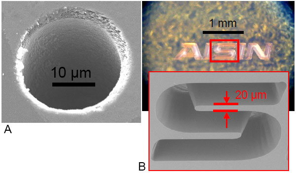
Figure 1: Laser micromachining examples in single-crystal diamond. A) 20 µm diameter hole B) 130 µm wide by 150 µm deep letter
Microelectronics in particular is one of the largest industry sectors that uses laser micromachining for a variety of applications including mask repair,1 chip repair, link-blowing, wafer processing, via-hole drilling and others. Pulsed lasers that are widely used include Excimer lasers and Q-switched solid-state lasers such as Nd:YAG and Vanadate systems. These conventional types of micromachining lasers typically produce pulses with durations of nanoseconds to microseconds. In the last several years however, femtosecond lasers have shown great promise to improve the quality and reduce the scale of fine detail which can be obtained by laser micromachining. The unique ablation properties of femtosecond lasers render higher precision in micromachining with reduced thermal effects, as well as a reduction in debris, recast, and burring. Additionally, they allow easier cutting and drilling of transparent materials with less collateral damage to the workpiece. This opens up possibilities to either replace conventional lasers in some applications, but there are also a huge variety of new emerging applications that will be enabled by these unique capabilities. These unique processing capabilities are being exploited in the semiconductor industry as well as the field of ophthalmic surgery. Several interesting potential application areas are discussed below.
Principle of Operation of Femtosecond Fiber Lasers
The remarkably clean ablation properties exhibited by ultrashort laser pulses stem from the extremely high peak power and short pulse duration, which ionizes and vaporizes materials quickly before thermal effects such as heat diffusion can occur.2 Because of this, the irradiated region of the target cannot lose its energy during the short time that the laser pulse is depositing energy in the material. This localizes the heating almost exclusively to the irradiated area, and thereby lowers the threshold for ablation. Not only this, but the heated and vaporized material is expelled quickly away before it can heat the neighboring areas of the target material. This results in a reduction of the heat-affected-zone (HAZ) and the shock-affected-zone (SAZ), as illustrated in Figure 2. Less material is melted and re-fused, resulting in less recast. Because the induced shock wave is also less intense, there is a reduction of the SAZ and less debris is scattered in the vicinity of the ablation zone. This clean ablation process allows extremely precise machining of micro-sized or even sub-micron sized structures by either direct-write or areal exposure techniques. It has been demonstrated in a spectacular way by the cutting and structuring of high explosive materials without detonation.3
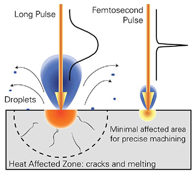
Figure 2: Comparison between long pulse and femtosecond pulse laser ablation.
Applicable Materials for Femtosecond Fiber Lasers
Another remarkable aspect of femtosecond laser ablation is that these clean ablation effects work for a wide variety of materials classes, whether they are metals, ceramics, semiconductors, dielectrics, or biological materials, cells, and tissues. For most laser micromachining, ablation works best when the material is absorbing at the laser wavelength, which is why, for example, Excimer lasers with UV output are used more commonly for machining ceramics and polymers and other materials which are transparent in the visible, but have some absorption in the UV. With femtosecond laser pulses of high intensity, it is possible to reproducibly and precisely machine transparent materials, even materials which are transparent to the laser wavelength. Even though the femtosecond laser pulse is usually in the IR (800 nm or 1060 nm typically) which is in the transparency region for many dielectrics, the high-speed, high-intensity pulses are equivalent to “UV on the target.” This stems from nonlinear optical effects in the materials which are driven by the extremely high intensities which are generated by amplified femtosecond laser systems. An ultrashort laser pulse having a pulse energy of Ep = 1 mJ and duration of 1 ps has a peak power of Ppeak = 1 MW. When this is focused onto a spot of size 5 mm the power density reaches levels of Ipeak ~ 1012 – 1013 W/cm2. At these intensities, multi-photon ionization strips the outer electrons from the constituent atoms of even transparent dielectric materials. This starts a cascade of avalanche ionization, leading to optical breakdown, and vaporization of the material. The result is a remarkably controlled and predictable ablation threshold and removal rate.
Comparison of Laser Systems for Micromachining
Typically, Ti:Sapphire lasers have been used for most micromachining applications, based on their established status in the research community. These systems have high energies of ~1 mJ with repetition rates of 1-5 kHz. However, for tightly focused beams, the 1 mJ pulse energy is far above the ablation threshold, and many of the advantages of the femtosecond laser are lost; i.e., there is an increase in thermal effects, with melting, recast, and debris generation unless the laser intensity is reduced to near-threshold. Usually, this results in most of the power being discarded and wasted. Additionally, the relatively low rep-rate does not lend itself well to direct-write micromachining techniques which often require rapid beam scanning by galvanometers. A higher repetition rate would be beneficial in such cases.
Fiber-based femtosecond lasers such as the IMRA’s FCPA µJewel provide an excellent alternative performance regime for micromachining. With 10 µJ pulses at repetition rates up to 1 MHz, the FCPA provides ample light intensity for ablation of most materials with a focused spot, and a high enough repetition rate for direct-write applications. Table 1 compares the performance of a typical Ti:Sapphire laser system and the predecessor of the FCPA µJewel, the FCPA-2 (first available for sale in 2001).
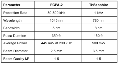
Table 1: Laser Performance Parameters
Parametric studies were performed by IMRA in 2004 comparing the ablation thresholds and material removal rates for the FCPA-2 fiber laser and a 1 kHz Ti:Sapphire regenerative amplifier system.5 Several materials were studied including metals, semiconductors, and dielectrics. Ablation threshold results are summarized in Table 2, where the repetition rates of the FCPA-2 laser and the Ti:Sapphire regenerative amplifier were set to 200 kHz and 1 kHz respectively.
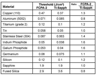
Table 2: Ablation Threshold Fluences
It was found that the thresholds for the two lasers are quite similar for most materials, with the 800 nm pulses from the Ti:Sapphire giving a slightly lower threshold. Figure 3 shows the dependence of the threshold on the repetition rate (that is, the pulse separation). The ablations threshold actually decreases as the pulse separation decreases, which means higher repetition rates are an advantage.
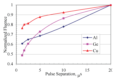
Figure 3: Normalized Threshold vs. Pulse Separation for three materials processed by the FCPA-2.
Sub-Diffraction-Limited Resolution
Some applications (mask repair for example), require spatial detail and resolution well below 1 micron. The well-defined ablation threshold and minimal thermal diffusion can be used to another advantage: sub-diffraction-limited resolution. The principle is illustrated in Figure 4. If a Gaussian beam profile is focused on the target, and the pulse energy is adjusted correctly, then only the intensity at the peak of the Gaussian will be above the ablation threshold, thus removing material from a spot which is smaller than the laser spot size itself. Initial demonstrations on thin silver films (600 nm thick) showed that it is possible to drill a hole with 300 nm diameter even though the laser spot size was 3 mm on target, and the wavelength was 800 nm.4 This capability will enable a number of machining applications which require extremely small feature sizes.
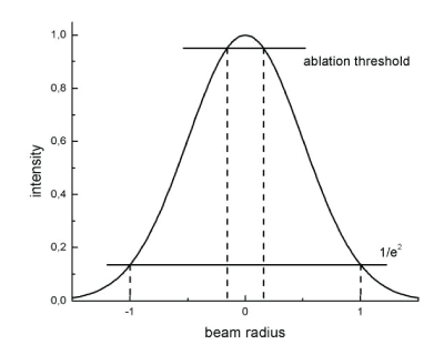
Figure 4: Schematic of the intensity distribution in the focus of a Gaussian laser beam. With careful adjustment of the pulse energy, only the fluence near the center of the beam is above the ablation threshold, making sub-diffraction-limited structuring possible.
Example 1: Thin Film Removal
Metal films on polymer substrates frequently require patterning with very fine detail, down to the micron scale. One method is to use chemical etching, which requires a multi-step lithography process. It would be convenient to use lasers for direct write patterning of the metal on the substrate. However, this is often difficult due to the fact that the polymer substrate usually has a lower melting point than the metal film on top of it.
When using CW lasers, it is virtually impossible to remove the metal without also damaging the substrate severely, as shown in Figure 5.A. Although the 5 mm thick metal film is removed, the spatial resolution is poor. When using femtosecond pulses as shown in Figure 5.B., the resulting lines are cleanly cut in the film with widths down to 8 mm or less. The high repetition rate (> 200 kHz) of the FCPA-2 laser greatly increases the linear speed of the direct-write process as compared with conventional Ti:Sapphire regenerative amplifiers having repetition rates of 1-5 kHz.
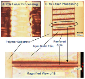
Figure 5: A) CW laser removal of metal film severely damages the polymer substrate. B) Femtosecond laser processing cuts clean lines into the metal film with minimal effect on the substrate.
Example 2: Surface Nanostructuring
Irradiation of polished surfaces by femtosecond laser pulses produces a periodically, nanostructured surface. The characteristics of the surface structure, such as the depth, periodicity, direction, and pattern, depend on the beam polarization, energy, and exposure, and can thus be controlled to some extent. This type of structure is known to reduce the friction between surfaces (supposedly by increased retention of lubricants) and is thus expected to be useful for a variety of mechanical parts.
Figure 6 shows the polarization dependence of the periodic surface structure formed on copper at a pulse fluence of F = 0.22 J/cm2. Note that for linear polarization, the machined surface ridges run perpendicular to the beam polarization. Use of circular polarization produces sub-micron sized conical structures.
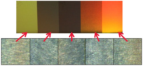
Figure 6: Nanotexturing on polished stainless steel coupons. The direction of the ridges is determined by the polarization of the incident laser beam.
Potential applications of nanostructuring include reduction of bearing friction, enhancement of the surface area of catalysts and engineering of surface-wetting properties.
Summary
Femtosecond laser pulses have demonstrated advantages over “long” (nanosecond or picosecond) laser pulses for many materials. The laser energy can be deposited rapidly, and is localized in the irradiated area without thermal diffusion to neighboring areas. This results in very clean ablation and precise, controllable material removal. Because of these advantages, ultrafast lasers are becoming the preferred lasers for applications in microelectronics and for ophthalmic surgery.
High-repetition rate, amplified femtosecond fiber lasers allow increased speed of direct-write processes such as thin film removal and also enable film removal which would be difficult or impossible by other means without damage to the surrounding areas. The example given above was for metal films on polymer substrates, but may also apply to industry-critical applications such as patterning of low-k dielectrics on semiconductors. Surface nanostructuring also has potential applications in all areas of mechanical part manufacturing as well as catalysis.
References
- Haight, D. Hayden, P. Longo, A. Neary, A. Wagner (1999). “MARS: Femtosecond laser mask advanced repair system in manufacturing,” J. Vac. Sci. Technol. B Vol. 17, pp. 3137-3143
- Nolte (2003) “Micromachining.” In M.E. Fermann, A. Galvanauskas, G. Sucha (Eds.), Ultrafast Lasers: Technology & Applications, pp. 359-394. New York, NY: Marcel Dekker Inc.
- D. Perry, B.C. Stuart, P.S. Banks, M.D. Feit, V. Yanovsky, A.M Rubenchik (1999). “Ultrashort-pulse laser machining of dielectric materials,” J. Appl. Phys. Vol. 85, pp. 6803-6810
- P. Pronko, S.K. Dutta, J. Squier, J.V. Rudd, D. Du, G. Mourou (1995). “Machining of sub-micron holes using a femtosecond laser at 800 nm,” Opt. Commun. Vol. 114, pp. 106-110
- Bovatsek, L.Shah, A. Arai, T. Yamamoto, Y. Uehara (2004). “Laser ablation threshold and etch rate comparison Between the ultrafast Yb fiber-based FCPA laser and a Ti:Sapphire laser for various materials,” Proc. SPIE Vol. 5662, pp. 661-666